Spintronics and its developments: material interfaces in the spotlight
These articles were originally published in L'Édition N.21.
For some time, new themes have been emerging in spintronics, exploring the original effects in nanometric heterostructures of involved materials and at their interfaces. They are studying its potential for the development of new spintronic devices that are not only even more efficient, but also and above all consume very little energy.
Magnonics, oxytronics, orbitronics... While the discovery of giant magnetoresistance by French physicists Albert Fert and German Peter Grünberg – awarded the Nobel Prize for Physics in 2007 – marked the birth of spintronics in 1988, today, this science combining electronics and magnetism is booming. Based on exploiting the spin of electrons – one of the elementary building blocks of atoms – since the late 1990s it has been the origin of the revolution in the information storage capacities of hard disks and the development of technologies involving the fine detection of magnetic current fields.
Today, the digital sector, whose technologies are mainly based on conventional electronics, accounts for 10% to 12% of global electricity consumption. With the explosion of cloud computing and data centres, this figure will possibly reach 20% - 30% by 2030. An environmental cost incompatible with global warming and the need for energy sobriety. Consequently, a paradigm shift is required: alternative, more energy efficient solutions for processing and storing information must be proposed. One of them is to use spintronic components, which are intrinsically much more energy-efficient.
At Université Paris-Saclay, several laboratories are involved in research that could lead to virtuous innovations. This is for example the case of the Joint Physics Unit CNRS/Thales (UMPhy – Univ. Paris-Saclay, CNRS, Thales), the Centre for Nanoscience and Nanotechnology (C2N – Univ. Paris-Saclay, National Centre for Scientific Research or CNRS, Univ. Paris Cité), the Condensed State Physics Service (SPEC - Univ. Paris-Saclay, CNRS, Alternative Energies and Atomic Energy Commission or CEA) and the Solid State Physics Laboratory (LPS – Univ. Paris-Saclay, CNRS). These teams, along with others, are working towards a better understanding of the physical effects operating in various materials and/or spintronics nanostructures, and are contributing to new cycles of innovations, as part of the SPIN priority research programme (see focus hereafter).
From a charge current to a spin current
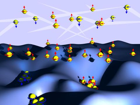
Spintronics is a recent research field that manipulates spin currents. Unlike conventional electronics, which relies solely on the electron’s negative electric charge and the manipulation of charge currents to process information, it relies additionally on one of the electron’s intrinsic properties, its spin (or magnetic moment), where only two orientations are possible: upwards (spin up) or downwards (spin down).
It started with the discovery of the giant magnetoresistance effect and the progress of ultra-thin film deposition techniques (a few nanometres thick). The basic concept is to place different layers of materials (alternating magnetic and non-magnetic materials) successively on the path of the electrons of a current, and to modify their electric resistance by applying a magnetic field, which changes the relative magnetisation of the magnetic layers. Ferromagnetic metals (iron, nickel, cobalt), which have an intrinsic magnetism, are used for this. The mobility of the electrons in the current flowing through such a layer depends on the orientation of the spins with respect to the magnetisation of the layer. It is greater if the spins are aligned (parallel orientation) rather than opposed (antiparallel orientation); the electrical resistance is low and high respectively. The resistance of a multilayer is then more or less important (or weak) according to the relative orientation of the magnetisation of the layers.
Magnetic tunnel junctions, in which an insulating layer separates two ferromagnetic layers of opposite orientation, are a flagship device developed on the same principle. They have been at the heart of hard disks for twenty years and are now essential elements of magnetic random access memories (MRAM), in which the information is coded and stored in binary form (0 or 1), depending on the alignment (parallel or antiparallel) of the magnetisations.
Couplings and memories
Another spintronic effect has been added to this landscape around the year 2000: spin-transfer torque (STT). With it, a spin-polarised electric current (or ideally a pure spin current), if large enough, is able to force the reversal of the magnetisation of the magnetic layer crossed.
Scientists are now evaluating the potential of other types of heterostructures, also involving ferroelectric or even multiferroic (ferromagnetic, ferroelectric and ferroelastic) materials. New effects are emerging, such as spin-orbit torque (SOT). This comes from the relativistic interaction between the magnetisation associated with the spin of the electron and the orbital motion of the electron. The interaction deviates the electrons from their trajectory in opposite directions for opposite spins. This provides for more efficient charge-to-spin current conversions. This effect is of particular interest when creating a new type of memory (SOT-MRAM).
It is also at the heart of a project involving UMPhy and the industrial company Intel which aims to develop a new type of transistor, the MESO (Magneto Electric Spin-Orbit Transistor). “The idea is to store information in a heterostructure where the input signal directs the polarisation of a multiferroic or magnetoelectric element coupled to a ferromagnetic element, to ‘write’ the magnetisation of the ferromagnetic element, and then ‘read’ this magnetisation by converting the spin current into a charge current,” explains Albert Fert, now Emeritus Professor at UMPhy. “The project with Intel aims for extremely low consumption levels, in the attojoule (10-18 joule) range.»
Interfaces show their potential
The surface of nanomaterials placed in heterostructures and their interfaces are also areas being studied. Particular relativistic interactions (Dzyaloshinskii-Moriya interaction or DMI, Rashba interfaces, etc.) generate original electronic and topological states. Some metal two-dimensional (2D) electron gases are therefore fascinating objects. They are created at the interface of insulating oxides such as strontium titanate (SrTiO3) or potassium tantalate (KTaO3). “These gases are very interesting because they have a very high mobility,” says Agnès Barthélémy, from the Oxytronics team at UMPhy. “When lanthanum aluminate (LaAlO3) is deposited on SrTiO3, a charge discontinuity is created at the interface, because the atomic planes of TiO2 and SrO are neutral and those of LaAlO3 are charged. If the LaAlO3 layers are further increased, a potential divergence is caused called polar catastrophe. To avoid this, a transfer of charges is made from the surface of the material to the interface, which creates a 2D electron gas. Another way to create the gas is to deoxidise SrTiO3 by sputtering a material such as aluminium at room temperature. The aluminium will pump oxygen from SrTiO3, reduce it and produce electron-donating oxygen vacancies.”
Magnetic textures, such as magnetic skyrmions are other objects that have recently been discovered. Long predicted, they were only observed for the first time about ten years ago. In these objects, the magnetic moments wrap around themselves in an arrangement topology stabilised by the DMI. This interaction requires two ingredients: symmetry breaking and spin-orbit coupling. “In spintronics, it is quite common to have fairly heavy materials, such as platinum or palladium, in which the spin-orbit coupling is strong. When we make stacks with layers of heavy materials in contact with thin magnetic layers, we obtain very strong DMI amplitudes at the interface, even promoting local rotations of the magnetic moments and generating a state that is energetically favourable to the appearance of skyrmions,” explains Vincent Cros of UMPhy.
These magnetic textures have a set of remarkable intrinsic properties. “They are often topologically non-trivial, stable and resistant to external perturbations. They are also very small in size: from a few nanometres to a few tens of nanometres. They also have electronic transport properties. With the help of spin currents, we can move them, guide them and make them interact,” comments Vincent Cros. This makes them interesting as a potential information carrier for new devices (memories, logic devices or even neuromorphic devices).
From domain walls to spin waves
Within the Novel Magnetic Devices (NOMADE) group at C2N, Thibaut Devolder and Joo-Von Kim’s research has long focused on domain walls, another magnetisation configuration in which to store information. “When you want to develop a memory, such as the now industrially mature STT-MRAMs, you need to understand beforehand how the wall moves, thus the magnetisation dynamics of the nanostructure, so that the switching time can be reproduced. However, when such an object moves, it is necessarily subject to friction, which opposes the movement. This friction can be deterministic (fluid, viscous) or involve the passage of obstacles,” comments Thibaut Devolder.
Recently, his team has been interested in the physics of spin waves and the means to generate, detect and manipulate these waves in nanostructured ferromagnetic metals. “These are magnetisation waves that propagate in time and space.” They have very original characteristics: “They are anisotropic (they display different properties depending on their direction of propagation), frequency-adjustable (their phase and frequency can be manipulated with an external stimulus), and non-linear (they easily interact with each other).” “This physical richness opens up new prospects for applications, especially in low-power embedded electronics. We expect applications in communication technologies, neuroinspired tasks, analogue calculation, pattern or voice recognition,” adds Joo-Von Kim.
As you can see, spintronics is booming. Moreover, as Albert Fert says with a smile in conclusion: “Each new direction explored opens up new ones. Science is always moving forward!”
Publications:
- Luis M. Vicente-Arche et al. Metal/SrTiO3 two-dimensional electron gases for spin-to-charge conversion. Phys. Rev. Materials 5, 064005 (2021).
- Grelier, M. et al. Three-dimensional skyrmionic cocoons in magnetic multilayers. Nat Commun 13, 6843 (2022).
- A. Mouhoub et al. Exchange energies in CoFeB/ Ru/CoFeB synthetic antiferromagnets. Phys. Rev. Materials 7, 044404 (2023).

The new generation of spintronic sensors, integrating innovative concepts and/or architectures, promise to be more agile, sensitive and robust, and lower the detection threshold of magnetic signals.
If there is one sector that has benefited from the development of spintronics, it is that of magnetic field sensors. “When spintronics started to arrive on the application bench, it all happened very quickly and today, many things are already being marketed. In the automotive sector, for example, spintronic technologies, which are more sensitive, easy to integrate and consume less energy, have supplanted other previously-used technologies,” notes Myriam Pannetier-Lecoeur, of the Nanomagnetism and Oxides Laboratory (LNO) of the Condensed State Physics Service (SPEC – Univ. Paris-Saclay, CNRS, CEA). “There are sensors for speed, position, angles, current, etc.”
Scientists are now looking at new features and adaptability. To do so, they rely on spin-transfer torque effects and magnetic textures, the potential of which is still to be fully explored. “We are trying to develop more dynamic and sensitive sensors, with sensitivity in all three dimensions of the space. We also want to make their properties changeable on demand under electrical control, if the environment and the magnetic field range change.”
Reducing sensor noise is another focus of research efforts. “A sensor always has a basic noise, related to the thermal agitation of electrons and related to the electrical resistance of the material. At low frequencies, a noise in 1/f is added, corresponding to fluctuations in different energy levels. To reduce it, either the magnetic effects must be stabilised or the volume of the device increased.”
Research at the interface with other sciences
Some of the group’s work concerns the detection of the magnetic signature of currents (neural, cardiac) in a body. “Very small and local, they create magnetic fields with a value several orders of magnitude below that of the Earth’s field (40 μT). To detect them, we need to increase the sensitivity of the sensors and decrease the noise.” Recently, the team has developed a sensor placed at the tip of a 25 μm probe to measure in vivo the signature of neurons in the hippocampus of rats. “A standard electrode records the electrical signal, which displays spikes in neuron activity. In parallel, the magnetic signal is recorded with the probe. Several one-hour sequences are carried out. After sorting and associating the electrical signals to the neurons near the probe, we match the magnetic acquisitions and average the events (several thousand!) to extract the magnetic signature of these neurons from the noise, in the order of nT,” explains Myriam Pannetier-Lecoeur. “With sensors that are ten times more sensitive, we would have a hundred times fewer events to average. This would save time and allow us to go further!”
Other work targets magnetic imaging, including the development of a magnetic microscope capable of observing magnetised objects. “We are also rolling out a low-field MRI project to be installed around the incubators of premature babies in hospitals. For these intermediate frequency (10 mT) signals, the coils of traditional MRI are less sensitive.” A striking fact: all these projects share a common denominator, dear to the team: to go as far as implementing the technology developed in real-life situations.
Publication :
- Chloé Chopin et al. Magnetoresistive Sensor in Two-Dimension on a 25 μm Thick Silicon Substrate for In Vivo Neuronal Measurements. ACS Sens. 2020, 5, 11, 3493–3500.
With a budget of just over 38 million euros over eight years, the SPIN Priority Research Programme and Equipment (PEPR) aims to promote a new cycle of innovation in spintronics, considering frugality as an essential criterion and equal to the computing power, speed, miniaturisation or cost of devices. As part of the “France 2030” investment plan, it involves more than forty laboratories in France.
“We have chosen subjects which, for us, define the important future focuses of spintronics and on which French teams are already working and at the forefront of research,” explains Vincent Cros, CNRS co-director of the PEPR SPIN with Lucian Prejbeanu from CEA. “The first three targeted projects concern topological textures, ultrafast or terahertz spintronics, and the dynamics of spin waves and magnonic effects. For these themes, the TRL (Technology Readiness Level) is relatively low (1 to 3). The other two targeted projects, which are a little more mature (TRL4), relate to spin transfer oscillators, for which there are still some obstacles to be removed, and spintronic sensors, one of the first flagship applications of spintronics, where we want to offer new-generation sensors with new functionalities and better properties.” The cross-functional platform projects target families of materials on which to conduct new research on spintronics, the tools for characterising their properties, and the theory-simulation, the objective of which is to structure the community. Two open calls for proposals, the first of which will be launched by late 2023/early 2024, will be used to complete the themes covered and set up interdisciplinary studies.
The targeted projects are exploratory, which is the very definition of this PEPR: “The choice was made to allocate significant resources to emerging but promising scientific themes so that these projects could then become part of the national strategy and be included in the acceleration PEPR.” There is already a very close link with the Electronics acceleration PEPR, “in which research in spintronics is integrated in order to develop new generations of spintronic memory.”